
Semicon Solutions from Panasonic
Looking for semicon solutions?
Semicon manufacturing requires precision solutions and Panasonic has products that will improve that process. Check out some selected possible applications of Panasonic products below. Don't see what you're looking for? Give us a call and we can help you with your application needs. 800-280-6933.
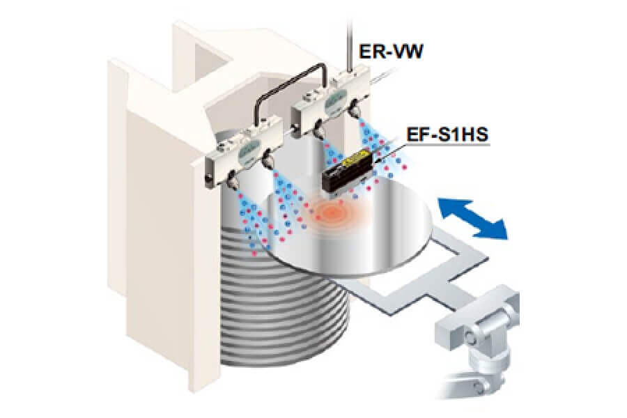
Surface potential measurement during loading and unloading
The sensor measures static electricity produced when transferring wafers and removes it with ionizers.
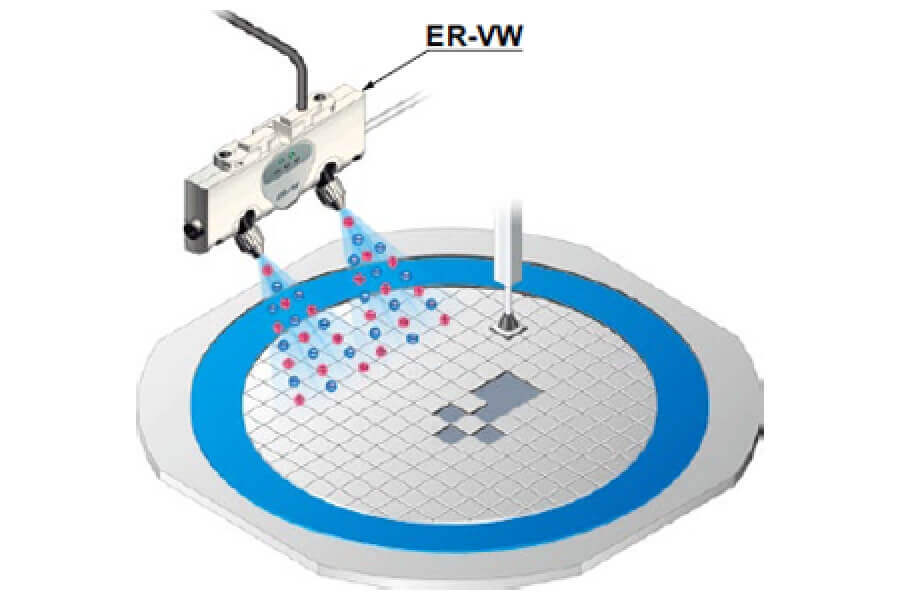
Removing charges during pickup from dicing tape
The thickness of the main body is 18.9 mm (0.744 in). In addition, the nozzle angle can be adjusted so that you can mount the ionizer inside a device, preventing device breakage due to static electricity.

Prevent static damage during bonding
Bare chips that have been cut from wafer during the dicing process are among the devices that are most susceptible to electrostatic damage. During bonding, it is recommended to reduce the charge to ±10 V or less through charge removal of small area with the ER-VS02.
Remove charges from adjacent lead from conveyor lines
The areas where electric charge will be removed can be designed according to the device since a maximum of five units can be connected.

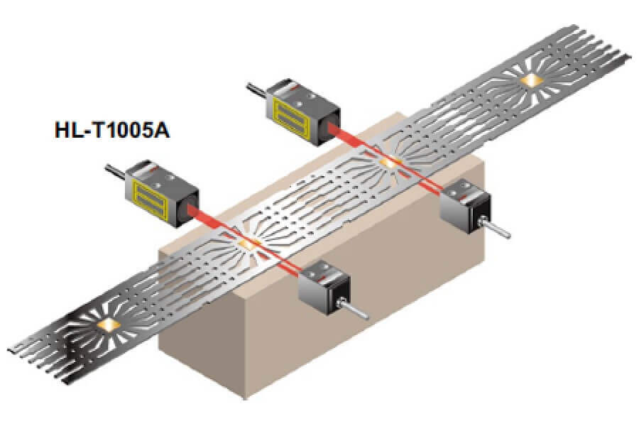
Detecting defective lead frame seating
A line light beam measures the slight protrusion of lead frames. It can verify before applying the mold press to prevent the flow of defective parts or damage to the mold.
Resin height inspection
HG-C is designed with a new optical system with a built-in mirror. It provides both industry's smallest class* form and high-precision measurement.
*Based on research conducted by our company as of March, 2014
